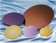
Base plates used for materials of optica communication components
光通信用の部品の材料として使用される基板
We are the first company nationwide specializing in a wide variety of film-forming processing on silicon wafers used for semiconductors and optical communication. Semiconductor industry has pursued thinner films on wafers up to several tens of nanometers. We focused attention on processing thick film by new thermal oxidation film processing. Our research and development enabled us to establish new technology to process and massproduce uniform and high-quality thermal oxidation films with the thickness of up to 25 micrometers. Maximum wafer size we can process is up to 12 inches.
当社は、半導体や光通信に用いられるシリコンウェーハ上に各種膜付加工を行う、日本国内初の成膜加工専門会社です。半導体業界などでは、ウェーハ上への加工膜について数十ナノメートルまで薄さが追及される中、当社は、新たな熱酸化膜加工による厚い膜の加工に着目しました。研究開発の結果、膜厚25マイクロメートルまでの均一で高品質な熱酸化膜を加工、量産できる技術を確立しました。ウェーハサイズは12インチまで加工が可能です。

Development, manufacturing, and marketing of a wide variety of film-forming processed products on silicon wafers for semiconductors and optical communication
半導体・光通信用シリコンウェーハ上の各種膜付加工品などの開発、製造、販売